XC5VSX95T-2FFG1136C Manufacturers

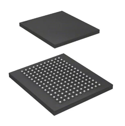
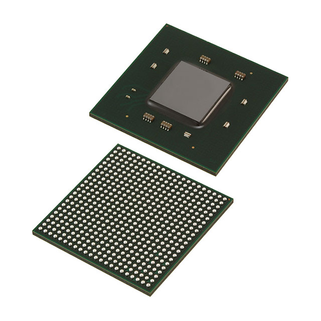
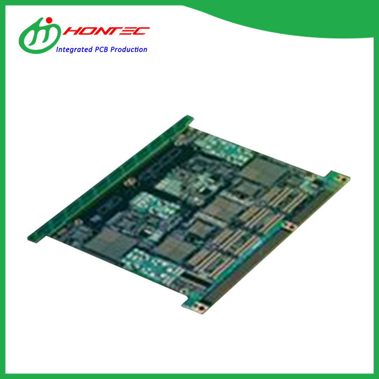
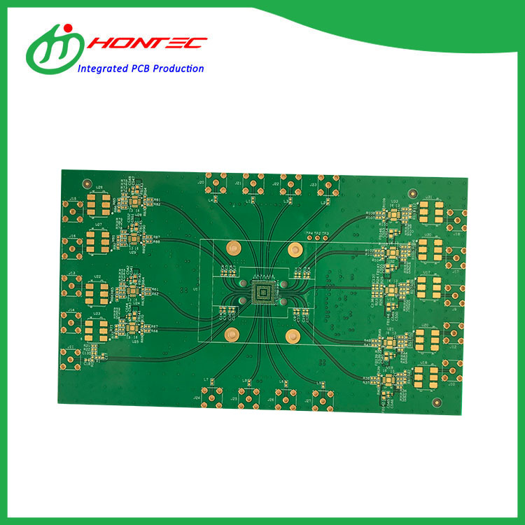
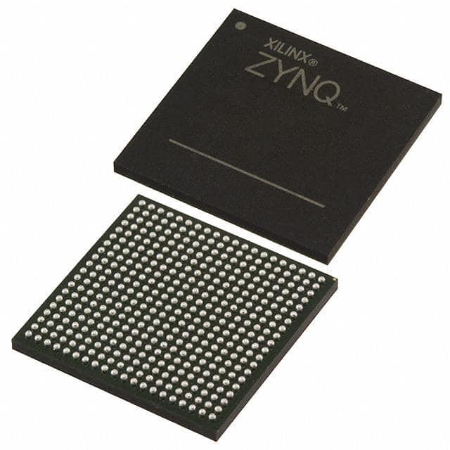
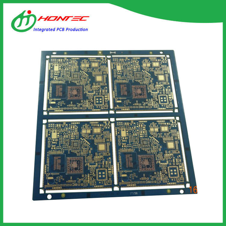
Bear "Customer very first, Quality first" in mind, we work closely with our customers and supply them with efficient and professional services for XC5VSX95T-2FFG1136C, If you're interested in any of our products and services, make sure you don't be reluctant to call us. We've been wanting to reply you within 24 several hours just after receipt of your respective ask for and to generate mutual un-limited positive aspects and enterprise in in the vicinity of long run.
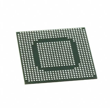
XC5VSX95T-2FFG1136C, Our mission is "Provide Merchandise with Reliable Quality and Reasonable Prices". We welcome customers from every corner of the world to contact us for future business relationships and achieving mutual success!

Hot Products

  • XC3SD1800A-4CSG484I

    XC3SD1800A-4CSG484I

    XC3SD1800A-4CSG484I is a high-performance field-programmable gate array (FPGA) developed by Xilinx, a leading semiconductor technology company. This device features 1.8 million system gates, 624 user input/ output pins, and 288 DSP slices, making it ideal for high-performance applications. It operates on a 1.2V to 1.5V power supply and supports various I/O standards such as LVCMOS, PCI, and SSTL. The device has a maximum operating frequency of 250 MHz.
  • 800G optical module PCB

    800G optical module PCB

    800G optical module PCB - at present, the transmission rate of global optical network is rapidly moving from 100g to 200g / 400g. In 2019, ZTE, China Mobile and Huawei respectively verified in Guangdong Unicom that single carrier 600g can achieve 48tbit / s transmission capacity of single fiber.
  • XCVU13P-2FHGA2104I

    XCVU13P-2FHGA2104I

    XCVU13P-2FHGA2104I is a scalable and reconfigurable acceleration platform suitable for optimizing complex workloads. It has a large amount of raw computing power and I/O flexibility, suitable for computationally intensive workloads in data center applications
  • LT3461ES6#PBF

    LT3461ES6#PBF

    LT3461ES6#PBF is suitable for use in a variety of applications, including industrial control, telecommunications, and automotive systems. The device is known for its easy-to-use interface, high efficiency, and thermal performance, making it an ideal choice for a wide range of power management applications.
  • Buried capacitance PCB

    Buried capacitance PCB

    24-Layer Buried capacitance PCB has a process called burying resistance, which is to put chip resistors and chip capacitors into the inner layer of the PCB board. These chip resistors and capacitors are generally very small, such as 0201, or even smaller 01005. The PCB board produced in this way is the same as a normal PCB board, but a lot of resistors and capacitors are placed in it. For the top layer, the bottom layer saves a lot of space for component placement. The following is about 24 Layer Buried capacitance PCB related, I hope to help you better understand 24 Layer Buried capacitance PCB.
  • Multilayer layers HDI PCB

    Multilayer layers HDI PCB

    Multilayer layers HDI PCB, press 3-6 layers first, then add 2 and 7 layers, and finally add 1 to 8 layers, a total of three times.The following is about 8 layers 3Step HDI, I hope to help you better understand 8 layers 3Step HDI.

Send Inquiry