Ro4730G3 PCB Manufacturers

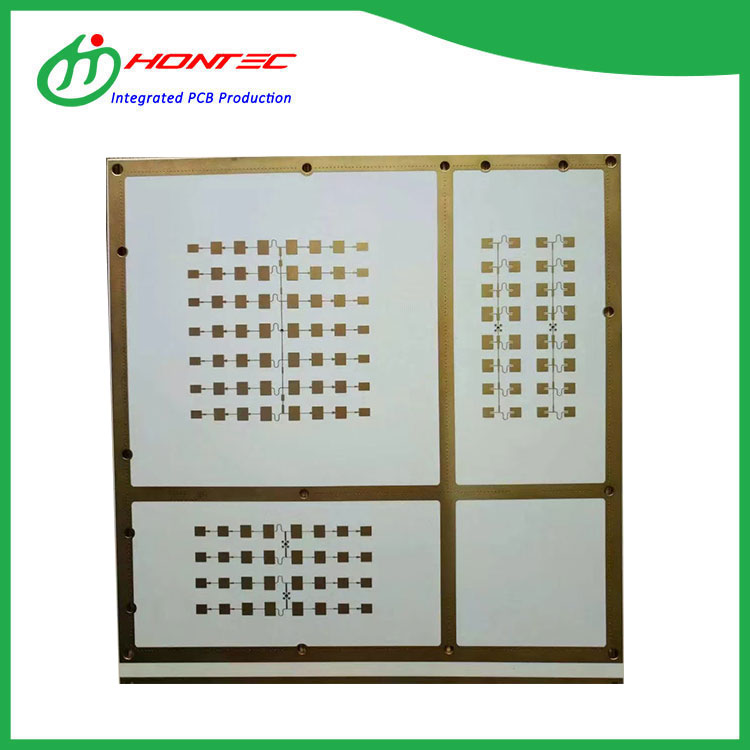
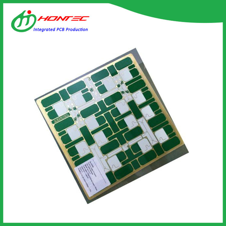
To be a result of ours specialty and repair consciousness, our corporation has won a good popularity amid consumers everywhere in the environment for Ro4730G3 PCB,Ro4003C PCB,Ro4350B PCB,Ro4360G2 PCB,Ro4533 PCB, We welcome an prospect to do small business along with you and hope to have pleasure in attaching further particulars of our merchandise.
Ro4730G3 PCB, Taking the core concept of "to be the Responsible". We will redound up on society for high quality solutions and good service. We are going to initiative to participate in international competition to be a first- class manufacturer of this product in the world.

Hot Products

  • 5AGXMA7G4F31C5G

    5AGXMA7G4F31C5G

    ​5AGXMA7G4F31C5G is a field programmable gate array (FPGA) with the following features: In addition, the product also has distributed RAM and embedded block RAM, with specific capacities of 15108 kbit and 1448 kbit, respectively. These features make 5AGXMA7G4F31C5G suitable for application scenarios that require high performance and high integration
  • 10M08DFV81I8G

    10M08DFV81I8G

    10M08DFV81I8G is a low-cost field-programmable gate array (FPGA) developed by Intel Corporation, a leading semiconductor technology company. This device features 120,000 logic elements and 414 user input/output pins, making it suitable for a wide range of low-power and low-cost applications. It operates on a single power supply voltage ranging from 1.14V to 1.26V and supports various I/O standards such as LVCMOS, LVDS, and PCIe. The device has a maximum operating frequency of up to 415 MHz. The device comes in a small fine pitch ball grid array (FGBA) package with 484 pins, providing high pin-count connectivity for a variety of applications.
  • Ladder PCB

    Ladder PCB

    Ladder PCB technology can reduce the thickness of PCB locally, so that the assembled devices can be embedded in the thinning area, and realize the bottom welding of ladder, so as to achieve the purpose of overall thinning.
  • Multilayer precision PCB

    Multilayer precision PCB

    Multilayer precision PCB--The manufacturing method of multilayer board is generally made by the inner layer pattern first, and then the single or double-sided substrate is made by printing and etching method, which is included in the specified interlayer, and then heated, pressurized and bonded. As for the subsequent drilling, it is the same as the plating through-hole method of double-sided board.
  • XCVU13P-2FHGA2104I

    XCVU13P-2FHGA2104I

    XCVU13P-2FHGA2104I is a scalable and reconfigurable acceleration platform suitable for optimizing complex workloads. It has a large amount of raw computing power and I/O flexibility, suitable for computationally intensive workloads in data center applications
  • XCVU9P-1FLGA2577I

    XCVU9P-1FLGA2577I

    XCVU9P-1FLGA2577I is suitable for use in a variety of applications, including industrial control, telecommunications, and automotive systems. The device is known for its easy-to-use interface, high efficiency, and thermal performance, making it an ideal choice for a wide range of power management applications.

Send Inquiry