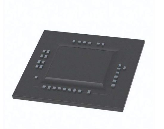
The XCVU7P-2FLVA2104I device provides the highest performance and integrated functionality on 14nm/16nm FinFET nodes. AMD's third-generation 3D IC uses stacked silicon interconnect (SSI) technology to break the limitations of Moore's Law and achieve the highest signal processing and serial I/O bandwidth to meet the strictest design requirements. It also provides a virtual single-chip design environment to provide registered routing lines between chips to achieve operation above 600MHz and provide richer and more flexible clocks.
The XCVU7P-2FLVA2104I device provides the highest performance and integrated functionality on 14nm/16nm FinFET nodes. AMD's third-generation 3D IC uses stacked silicon interconnect (SSI) technology to break the limitations of Moore's Law and achieve the highest signal processing and serial I/O bandwidth to meet the strictest design requirements. It also provides a virtual single-chip design environment to provide registered routing lines between chips to achieve operation above 600MHz and provide richer and more flexible clocks.
Application:
Calculation acceleration
5G baseband
Wired communication
radar
Testing and measurement
Product attributes
Device: XCVU7P-2FLVA2104I
Product type: FPGA - Field Programmable Gate Array
Series: XCVU7P
Number of logic components: 1724100 LE
Adaptive Logic Module - ALM: 98520 ALM
Embedded memory: 50.6 Mbit
Number of input/output terminals: 884 I/O
Power supply voltage - minimum: 850 mV
Power supply voltage - maximum: 850 mV
Minimum working temperature: -40 ° C
Maximum working temperature:+100 ° C
Data rate: 32.75 Gb/s
Number of transceivers: 80
Installation style: SMD/SMT
Package/Box: FBGA-2104
Distributed RAM: 24.1 Mbit
Embedded Block RAM - EBR: 50.6 Mbit
Humidity sensitivity: Yes
Number of logical array blocks - LAB: 98520 LAB
Working power supply voltage: 850 mV