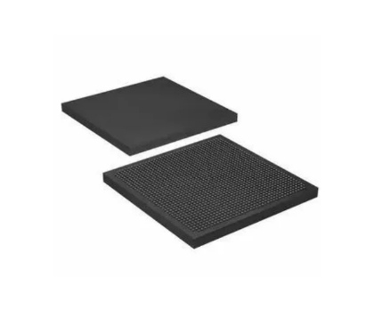
The XCKU115-3FLVF1924E field programmable gate array can achieve extremely high signal processing bandwidth in mid-range devices and next-generation transceivers. FPGA is a semiconductor device based on a configurable logic block (CLB) matrix connected through a programmable interconnect system
The XCKU115-3FLVF1924E field programmable gate array can achieve extremely high signal processing bandwidth in mid-range devices and next-generation transceivers. FPGA is a semiconductor device based on a configurable logic block (CLB) matrix connected through a programmable interconnect system. Can be used for packet processing in 100G networks and data center applications. They are also highly suitable for DSP intensive processing required for next-generation medical imaging, 8k4k video, and heterogeneous wireless infrastructure. Optimized for 20nm system performance and integration, utilizing single-chip and next-generation stacked silicon interconnect (SSI) technology.
characteristic
● Programmable System Integration
Up to 1.5M system logic unit, using second-generation 3D IC
Multiple integrated PCI Express ® Gen3 kernel
● Improve system performance
8.2 TeraMAC DSP computational performance
High utilization rate increases speed by two levels
Each device has up to 64 16G transceivers that support backplanes
2400Mb/s DDR4, capable of stable operation under different PVT conditions
● Reduced BOM costs
High system integration, reducing application BOM costs by up to 60%
● 12.5Gb/s transceiver with minimum speed equal polarity
Medium speed level can support 2400Mb/s DDR4
VCXO integration can reduce the cost of clock components